ΚΟΥΤΡΟΥΜΠΑΣΔΗΜΗΤΡΗΣ

Sunday, April 28, 2019
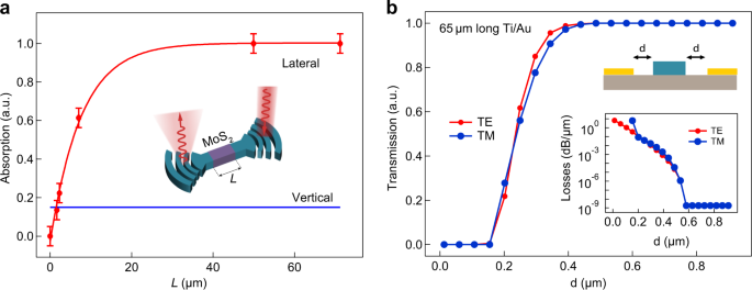
Εικ. 1 Φωτοανιχνευτής βασισμένος σε MoS 2 ενσωματωμένος σε ένα φωτονικό κύκλωμα. μια εγκάρσια διατομή του φωτοανιχνευτή, με μονοστοιβάδα MoS 2 απευθείας απολεπισμένη στην κορυφή του κυματοδηγού. b Υπολογισμένο μέγεθος πεδίου TE | E | για τον κυματοδηγό Si 3 N 4 . Το πελώριο πεδίο που επικαλύπτεται επικαλύπτεται με τη μεταφερόμενη νιφάδα MoS 2 . c Σχηματικά της σύζευξης φωτός με εστίαση ενός λέιζερ CW 647 nm στο φράγμα διάθλασης. Το φως διαδίδεται μέσω του κυματοδηγού Si 3 N 4 (WG) και δημιουργεί ζεύγη ηλεκτρονίων-οπών (eh) στο MoS 2 , το οποίο οδηγεί σε παραγωγή φωτοβολίδων στο πολωμένο MoS 2μονοστιβάδα. d Οπτική εικόνα του κατασκευασμένου φωτοανιχνευτή MoS 2 ενσωματωμένου στη φωτονική δομή. Το κανάλι MoS 2 επισημαίνεται σε βιολετί. Χρησιμοποιείται επίσης ο συζεύκτης σχάσης διάθλασης (GC) που χρησιμοποιείται για την ελαφριά σύζευξη, την πηγή κυματοδηγού (WG) και την αποστράγγιση. Η κλίμακα κλίμακας είναι 20 μm. Τα ένθετα παρουσιάζουν μια εικόνα φωτοφωταύγειας μονοστοιβάδας MoS 2 μετά την εικόνα και την ηλεκτρονική μικροσκοπία σάρωσης ηλεκτρονίων (SEM) του WG με GC. Η κλίμακα κλίμακας είναι 10 μm και για τα δύο ένθετα Εικόνα πλήρους μεγέθους Περιορισμένη απορρόφηση του προσπίπτοντος φωτός κανονικά σε 2D υλικά λόγω της ατομικής κλίμακας τους πάχους 23μπορεί να ξεπεραστεί με πλευρική διέγερση μέσω του κυματοδηγού. Για να καταδειχθεί αυτή η πειραματικώς, μετράται η πλευρική απορρόφηση του MoS 2 ως συνάρτηση του μήκους των νιφάδων. (Βλέπε Μεθοδολογία). Το Σχήμα 2α δείχνει ότι η πλευρική απορρόφηση υπερβαίνει την όρθια οντότητα (που λαμβάνεται από την Αναφ.16) και πλησιζει την μοναδα. Από μια εκθετική προσαρμογή της μετάδοσης ( Τ = e - L / α ), ο συντελεστής απορρόφησης βρέθηκε να είναι α = 7.7 ± 1.1 μm. Είναι σαφές ότι η πλευρική απορρόφηση μπορεί να τελειοποιηθεί τροποποιώντας το μήκος της νάφτας, η οποία θα μπορούσε να καθοριστεί από ένα πρόσθετο βήμα μετά την μεταφορά. Σχ. 2 Εικ. 2 Η επίδραση της μονοστοιβάδας MoS 2 και οι μεταλλικές επαφές διάδοσης του φωτός εντός του κυματοδηγού. μια σύγκριση μεταξύ MoS 2 πλευρικής (πειραματικά σημεία δεδομένων) και κατακόρυφης απορρόφησης (που λήφθηκαν από την Αναφ.16) ως συνάρτηση του μήκους των νιφάδων. Οι ράβδοι σφάλματος αντιπροσωπεύουν την τυπική απόκλιση των μετρήσεων. β υπολογίζεται σε σχέση μετάδοσης για ΤΕ (κόκκινο) και TM (μπλε) τρόπους μετά την απογραφή των 65 μm μακριών μεταλλικών επαφών σε απόσταση d από τον κυματοδηγό. Ένθετο δείχνει τις υπολογιζόμενες απώλειες ανά μικρομέτρο σε λογαριθμική κλίμακα Εικόνα σε πλήρες μέγεθος Για την οπτολεκτρονική περιγραφή του κυματοδηγού-ολοκληρωμένου φωτοανιχνευτή, η ποσότητα του φωτός που προσβάλλεται επί της διάταξης πρέπει να ποσοτικοποιηθεί. Εμπλουτισμένες Εικόνες S4 = 65 μm) επιλέγονται προκειμένου να μεγιστοποιηθεί το μήκος του καναλιού και μετά τη μεταβίβαση των μεγάλων μονοστοιχείων MoS 2 επί της επιφάνειας του κυματοδηγού και της σύζευξης με το περιβάλλον Si 3 N 4 στρώμα μπορεί να αγνοηθεί του κυματοδηγου. Για την ακρίβεια σε αποστάσεις μεγαλύτερες από 600 nm, η επίδραση των μεταλλικών επαφών στη διάδοση του φωτός είναι αμελητέα.), Η αλληλεπίδραση του φωτός με τις εξατμίστηκε μεταλλικές επαφές μπορεί να μεταβάλει τη διάδοσή του. Προκειμένου να μεγιστοποιηθεί η φωτορεύματος στο κατασκευασμένων φωτοανιχνευτή, οι επαφές θα πρέπει να είναι όσο το δυνατόν πλησιέστερα προς τον κυματοδηγό έτσι ώστε να μειωθεί η αντίσταση της συσκευής. Ωστόσο, αυτό μπορεί να τροποποιήσει διάδοσης του φωτός, αν οι αποσβένον ζευγάρια πεδίου στις μεταλλικές επαφές, οδηγώντας σε οπτικές απώλειες στον κυματοδηγό. Για να βρείτε την ελάχιστη απόσταση μεταξύ της πηγής και η διαρροή για τα οποία δεν μεταβάλλονται ΤΕ και ΤΜ προφίλ λειτουργίας, εκτελούμε προσομοιώσεις FDTD για τις διαφορετικές θέσεις των επαφών σε σχέση με τον κυματοδηγό. Σχετική μετάδοσης για αμφότερους τους τρόπους ΤΕ και ΤΜ μετά την εναπόθεση των 10 nm Ti, 60 nm Au φαίνεται στο Σχ. 2β . Το ένθετο παρουσιάζει απώλειες διάδοσης σε λογαριθμική κλίμακα. Long επαφές ( LΩς εκ τούτου, σχεδιάζουμε επαφές με 700 διαχωρισμό nm για να αποκλείσουμε την επίδραση της σύζευξης φωτός στο μέταλλο. Optoelectronic measurements are performed in vacuum (10−6 mbar) at room temperature, under continuous-wave (cw) laser illumination at a wavelength λ = 647 nm, unless stated otherwise. The three main mechanisms for photocurrent generation in MoS2 are photogating, photoconductive, and photothermoelectric effects.24,25 In our case, photogating is dominant, leading to a slow photocurrent ~80 times higher than the fast photocurrent associated with the photoconductive effect25 (see Supplementary Section 4). Photothermoelectric current can be neglected, since no appreciable current is measured at zero bias under light illumination (Supplementary Fig. S7). Figure 3a shows the schematics of the device band alignment in three different conditions: dark (1), vertical illumination (2), and lateral illumination via the waveguide (3), leading to the corresponding Ids−Vg curves in Fig. 3b. In the dark, current follows the characteristic behavior of an MoS2 transistor,12 with a threshold voltage Vth = −11 V and an on/off ratio above 105, limited by the noise level of the measurement setup. When focusing the laser light onto the flake, electron-hole (e-h) pairs are generated across the channel. The device stays in the on-state for the entire range of back-gate voltages, with trapped holes shifting the Fermi level, effectively gating the flake. Since the lifetime of trapped holes is much larger than that of the electrons, many carriers can flow for each generated e-h pair, resulting in a large photogain. The ratio of photocurrents under vertical illumination and in dark reaches values as high as Iflake/Idark > 6·103 at Vg = −12 V and is again limited by the noise level. When the flake is excited through the waveguide by focusing the laser on the grating coupler, creation of e-h pairs occurs only in the overlapping region between the waveguide and the flake, creating a potential profile for electrons which allows turning off the photocurrent. The off-state for lateral illumination is found at a new threshold voltage Vg = −37.5 V. Fig. 3 Εικ. 3 Optoelectronic properties of the device at room temperature. a Schematics of band alignment for device under applied bias in different conditions: dark (1), vertical (2) and lateral illumination (3). b Drain-source current (Ids) dependence on the applied back gate voltage (Vg) for the three regimes represented in a obtained at bias voltage Vds = 1 V and laser power Plaser = 25 nW. c Modulation of the photoresponse with back-gate voltage for lateral and vertical illumination at Vds = 1 V and Plaser = 25 nW. Responsivity is normalized by its value at zero gate voltage. d Measured photoresponsivity R as a function of incident power Pin at Vg = 0 V and Vds = 1 V. e Responsivity dependence on the excitation wavelength, normalized by its value at 647 nm (wavelength used for measurements shown in b, c, and photoluminescence spectra from MoS2 on Si3N4 Full size image From the Ids−Vg curves, we can further derive the external responsivity of the photodetector, defined as the ratio between the generated photocurrent Iph = Ilight − Idark and optical power Pin incident to the flake. Figure 3c shows the dependence of the photoresponse on the gate voltage for a fixed laser power of 25 nW. Due to the characteristic band alignment, in the case of lateral coupling the gate modulation of photoresponsivity is three orders of magnitude larger compared to vertical illumination, with responsivity dropping to zero for back-gate voltages below the threshold voltage. Dependence of responsivity on incident optical power at Vg = 0 V is shown in Fig. 3d. The responsivity for the waveguide is calculated by taking into account that the grating coupler efficiency is 3.4% at 647 nm wavelength (see Supplementary Section 6), so that Pin ~ 0.034 × Plaser. For low incident power we obtain an extremely high photoresponse above 1000 A/W, which is the result of higher lateral absorption compared to vertical illumination. Flake responsivity depends strongly on the excitation wavelength, as shown in Fig. 3e, and can be further enhanced by increasing the energy of incident photons. Photoresponse for wavelengths below the optical bandgap vanishes, as photons cannot be absorbed by the 2D material. It should be noted that photoresponse depends directly on the conductivity of the channel, and therefore slightly varies with time since MoS2 is known to experience Fermi level shifts on substrates such as SiO2 and S3N4 upon thermal, light or current annealing.26 The realization of chip-integrated devices with TMDCs requires precise alignment of light sources, such as optical fibers or lasers, on the material. However, relaxed alignment conditions can be achieved with the usage of grating couplers. Figure 4 presents photocurrent maps for vertical illumination on MoS2 and the grating coupler when a DC bias is applied to MoS2. For the latter, the map represents the spatial distribution of the coupling efficiency since it shows the photocurrent generated in the MoS2 when the light from the laser is focused onto the diffraction grating, then coupled to the waveguide and finally absorbed in the MoS2 layer (Supplementary Section 5). For the diffraction grating, significant photoresponse (>1/2 Imax) can be obtained over a larger area compared to the flake. In addition, response is homogeneous around the grating lines, which indicates that alignment could be greatly facilitated by simply increasing the diffraction grating area. The flake photocurrent map reveals an active channel length L ~14 μm, which corresponds to a lateral absorption of 84%, according to measurements presented in Fig. 2a. This leads to an external quantum efficiency for photons traveling in the waveguide ηext = 0.84. Photogain can then be calculated as 𝐺=𝑅×ℎ𝜐/𝑞𝜂ext> 2300, for low incident powers, where hυ is incident photon energy and q is the elementary charge. Fig. 4 Σχήμα 4 Normalized photocurrent maps for the case of direct vertical excitation on the flake (a) and excitation through the grating coupler (b) at Vds = 2 V, Vg = 0 V and laser power of 1 µW and 110 µW, respectively. Laser light is modulated using the chopper with a frequency of 30 Hz. The value of alternating current (AC) at the modulation frequency of light is obtained by a lock-in amplifier. Scale bar is 5 µm. Dashed lines denote the contacts in a and the outline of the grating coupler in b Full size image The main limitation of MoS2-based photodetectors is the low speed of operation, which in our case is restricted by the photocurrent rise and decay times 𝜏rise > 13s and 𝜏decay > 11s, respectively (Supplementary Fig. S6a). These slow response times are associated with the photogating mechanism which manifests itself as a change in the threshold voltage due to charge transfer to adjacent molecules, in particular when transferred onto SiO225 or Si3N4, as in our case. On the contrary, fast response is related to photoconductive and photoelectric effects.25 In order to avoid photogating and realize a device with a fast response, an alternative device is fabricated, where a multilayer h-BN flake with a thickness of ∼11 nm is first transferred on top of the waveguide, which serves as the van der Waals (vdW) substrate for MoS2 (Supplementary Fig. S8). We expect similar response time for vertical and lateral illumination via the waveguide, since the response time is associated with the mechanism responsible for photocurrent generation. This mechanism is the same regardless of whether we excite locally (waveguide coupling) or over the entire active area (vertical illumination), since the MoS2 flake is supported by a flat and homogeneous h-BN layer. When illuminating with a continuous wave laser, a constant photocurrent is generated. After adding a chopper rotating at 20 Hz at the output of the laser, the response of the device is still fast enough to reach maximum (constant illumination) and minimum (dark) values of photocurrent, which demonstrates that all the response is faster than 20 Hz. To determine more precisely the speed of the response, photocurrent is measured as a function of the chopper rotation frequency. Figure 5a shows the ratio between DC photocurrent (IDC) obtained for constant illumination, and oscillating photocurrent (IAC) at the frequency of the chopper, measured by the lock-in amplifier. The oscillating (fast) photocurrent is constant for frequencies of up to 1 kHz, the limit of the measurement setup. The response time of the monolayer MoS2/h-BN photodetector is therefore shorter than 1 ms, overcoming the performance of previously reported MoS2 photodetectors.27 Similar results are obtained when exciting via the waveguide, with lower photocurrents due to weaker coupling after the addition of thick h-BN, leading to a fast responsivity of 1.5 μA/W at Pin = 7 mW (Fig. 5a, inset). Fig. 5 Εικ. 5 Fast response and low-power operation of MoS2-based photodetectors. a Fast operation of the MoS2/h-BN photodetector: Lock-in amplifier measurements of AC photocurrent dependence on chopper frequency at Pin = 7 mW, Vg = 0 V and Vds = 1 V, under vertical illumination. Inset shows schematic structure of the photodetector and operation under dark (OFF) and chopped illumination at 1 kHz (ON) on the grating coupler with Pin = 7 mW, Vg = 0 V and Vds = 1 V. b Low voltage operation of the MoS2/h-BN/Gr photodetector. Main graph shows Ids−Vg curves under dark and illumination at Pin = 11 mW and Vds = 250 mV, showing low threshold voltage Vth = −250 mV without illumination. Inset graph shows Ids−Vds curves with and without illumination for Pin = 11 mW, Vg = −500 mV. Inset schematic depicts the structure of the photodetector Full size image For low-power applications of integrated optoelectronic devices, operation voltages need to be decreased. In order to have more efficient electrostatic control over the charge carrier density in the MoS2 flake, we fabricate a third device where multilayer graphene is used as a back gate, with an 11 nm thick h-BN dielectric layer. Resulting Ids−Vg curves for the device in the dark and under vertical illumination are shown in Fig. 5b. The off state is reached at a back gate voltage as low as Vg = −250 mV, due to the higher capacitance (C = 2800 μF/m2) of the thin h-BN dielectric compared to the 1 µm thick SiO2 (C = 34.5 μF/m2). High values of photocurrent on the order of µA can be measured for the complete range of back gate voltages. Figure 5b inset presents measured Ids−Vds curves in the off state, with gate voltage below the threshold. Photocurrent to dark current ratio over 105 is achieved at Vds = 300 mV and incident power of 11 mW. In summary, we demonstrate the integration of MoS2 photodetectors on photonic structures, and present device architectures for practical optoelectronic circuits. The first figure of merit is the large responsivity of the photodetector for lateral illumination at wavelengths close to the optical bandgap. Light emission from MoS2 at these wavelengths has already been demonstrated17 and therefore a platform for light emission and detection with monolayer MoS2 could be potentially realized. In addition, photocurrent can also be suppressed for gate voltages below a given threshold, leading to three different regimes in photoresponse. Homogeneous and large coupling area in the diffraction gratings facilitates alignment for future optical interconnects. Furthermore, by realizing more complex structures we demonstrate potential of this device as a platform for the development of MoS2-based integrated photodetectors aiming at various applications. In a second device, photoresponse times below 1 ms can be achieved by adding an h-BN layer between MoS2 and Si3N4. The use of a graphene back gate with thin h-BN as the dielectric in a third device reduces the voltage range needed to operate the phototransistor. Altogether, results from this work rise the prospects of MoS2 as a promising material for future integrated optoelectronic circuits. Methods Device fabrication Degenerately doped silicon wafers with 250 nm/1 µm Si3N4/SiO2 layers grown by low pressure chemical vapor deposition (LPCVD) were used for device fabrication. The thickness of SiO2 is high enough to decouple waveguide modes from the optically dense substrate. Photonic structures were patterned using electron beam lithography after spin coating of ZEP, followed by dry etching with CHF3/SF6. The polymer was then removed using O2 plasma and the resulting structure was submerged in KOH to smooth the waveguide sidewalls. Dimensions of photonic circuits were optimized for wavelengths at the MoS2 excitonic resonance, so that it can also be used for transmission of light emitted by MoS2-based devices. We further confirmed resulted dimensions of fabricated structures by scanning electron microscopy (SEM), focused ion beam (FIB) and atomic force microscopy (AFM), as shown in Supplementary Fig. S1. Calculated electric field profile for fundamental TE and TM mode based on FDTD simulations is plotted in Supplementary Fig. S2. Ultrathin layers of MoS2 were obtained by mechanical exfoliation with low residue tape. Monolayers are then deposited on visco-elastic films with a polyethylene coversheet (Gel-Pak) and peeled-off slowly. The contrast of monolayer flakes under the optical microscope has been calibrated and confirmed by atomic force microscopy (AFM) and photoluminescence (PL) measurements. Finally, polymer films were placed on a glass slide for dry transfer on top of the photonic structure. Post-transfer thermal annealing was done at 250 °C under high vacuum (10−7 mbar) for 6 h. The resulting structure was spin coated with PMMA A2/MMA EL6 and patterned by electron beam lithography, followed by electron beam evaporation of 10 nm Ti and 60 nm Au. Standard lift-off process with acetone was used for polymer removal. Figure S3 shows optical images of the device after different fabrication steps. Photoluminescence after annealing of the transferred MoS2 monolayer decreases significantly, with the suppression of exciton states due to charge transfer from the substrate, as shown in Supplementary Fig. S3c. Setup for optoelectronic measurements The bias voltages were supplied by a Keithley 2400 measurement unit which was also used for current measurements. Unless otherwise specified, all optoelectronic measurements were performed in vacuum (10−6 mbar) at room temperature, with a continuous wave laser illumination at 647 nm. The setup for optoelectronic measurements is presented in Fig. S5. Laser light is directed towards the sample by the beam splitter BS1, and the focus position is set by a piezoelectric stage mounted to the ×50 objective with a numerical aperture NA = 0.65. Light reflected or re-emitted from the sample is split by BS2 and collected by the CCD camera (Andor Ixon) and the spectrometer (Andor Newton). Determination of waveguide losses and MoS2 absorption For measurement of waveguide losses and MoS2 absorption, laser light with a wavelength of 647 nm is focused on the input grating, and light emission from the output grating is quantified with the number of counts measured in the CCD camera. By comparing counts measured for a reference structure, waveguide losses and MoS2 absorption can be extracted. In order to remove the reflected light, a cross-polarization scheme was used. Laser light is first polarized along the grating coupler lines, and the waveguide makes a turn so that emitted light in the output grating is polarized perpendicularly to incident light (see right inset in Fig. S5). Since the polarization of reflected light is the same as for incident light, we can remove laser reflection without affecting light emission form the output grating. Data availability The data that support the findings of this study are available from the corresponding author on reasonable request. Additional information Publisher’s note: Springer Nature remains neutral with regard to jurisdictional claims in published maps and institutional affiliations. References 1. Gurrum, S. P., Suman, S. K., Joshi, Y. K. & Fedorov, A. G. Thermal issues in next-generation integrated circuits. IEEE Trans. Device Mater. Reliab. 4, 709–714 (2004). Show context for reference 1 Article Google Scholar 2. Rickman, A. The commercialization of silicon photonics. Nat. Photonics 8, 579–582 (2014). Show context for reference 2 CASArticle Google Scholar 3. Moss, D. J., Morandotti, R., Gaeta, A. L. & Lipson, M. New CMOS-compatible platforms based on silicon nitride and Hydex for nonlinear optics. Nat. Photonics 7, 597–607 (2013). Show context for reference 3 CASArticle Google Scholar 4. Miller, D. A. B. Device requirements for optical interconnects to silicon chips. Proc. IEEE 97, 1166–1185 (2009). Show context for reference 4 CASArticle Google Scholar 5. Miller, D. A. B. Rationale and challenges for optical interconnects to electronic chips. Proc. IEEE 88, 728–749 (2000). Show context for reference 5 Article Google Scholar 6. Sun, Z., Martinez, A. & Wang, F. Optical modulators with 2D layered materials. Nat. Photonics 10, 227–238 (2016). Show context for reference 6 CASArticle Google Scholar 7. Bertolazzi, S., Brivio, J. & Kis, A. Stretching and breaking of ultrathin MoS2. ACS Nano 5, 9703–9709 (2011). Show context for reference 7 CASArticle Google Scholar 8. Akinwande, D. et al. A review on mechanics and mechanical properties of 2D materials—graphene and beyond. Extrem. Mech. Lett. 13, 42–77 (2017). Show context for reference 8 Article Google Scholar 9. Schwierz, F. Graphene transistors. Nat. Nanotechnol. 5, 487–496 (2010). Show context for reference 9 CASArticle Google Scholar 10. Gan, X. et al. Chip-integrated ultrafast graphene photodetector with high responsivity. Nat. Photonics 7, 883–887 (2013). Show context for reference 10 CASArticle Google Scholar 11. Bonaccorso, F., Sun, Z., Hasan, T. & Ferrari, A. C. Graphene photonics and optoelectronics. Nat. Photonics 4, 611–622 (2010). Show context for reference 11 CASArticle Google Scholar 12. Radisavljevic, B., Radenovic, A., Brivio, J., Giacometti, V. & Kis, A. Single-layer MoS2 transistors. Nat. Nanotechnol. 6, 147–150 (2011). Show context for reference 12 CASArticle Google Scholar 13. Wang, Q. H., Kalantar-Zadeh, K., Kis, A., Coleman, J. N. & Strano, M. S. Electronics and optoelectronics of two-dimensional transition metal dichalcogenides. Nat. Nanotechnol. 7, 699–712 (2012). Show context for reference 13 CASArticle Google Scholar 14. Mak, K. F. & Shan, J. Photonics and optoelectronics of 2D semiconductor transition metal dichalcogenides. Nat. Photonics 10, 216–226 (2016). Show context for reference 14 CASArticle Google Scholar 15. Splendiani, A. et al. Emerging photoluminescence in monolayer MoS2. Nano Lett. 10, 1271–1275 (2010). Show context for reference 15 CASArticle Google Scholar 16. Mak, K. F., Lee, C., Hone, J., Shan, J. & Heinz, T. F. Atomically thin MoS2: a new direct-gap semiconductor. Phys. Rev. Lett. 105, 136805 (2010). Show context for reference 16 Article Google Scholar 17. Lopez-Sanchez, O. et al. Light generation and harvesting in a van der Waals heterostructure. ACS Nano 8, 3042–3048 (2014). Show context for reference 17 CASArticle Google Scholar 18. Lopez-Sanchez, O., Lembke, D., Kayci, M., Radenovic, A. & Kis, A. Ultrasensitive photodetectors based on monolayer MoS2. Nat. Nanotechnol. 8, 497–501 (2013). Show context for reference 18 CASArticle Google Scholar 19. Bie, Y.-Q. et al. A MoTe2-based light-emitting diode and photodetector for silicon photonic integrated circuits. Nat. Nanotechnol. 12, 1124–1129 (2017). Show context for reference 19 CASArticle Google Scholar 20. Unuchek, D. et al. Room-temperature electrical control of exciton flux in a van der Waals heterostructure. Nature 560, 340 (2018). Show context for reference 20 CASArticle Google Scholar 21. Zhao, W. et al. Large area growth of monolayer MoS 2 film on quartz and its use as a saturable absorber in laser mode-locking. Semicond. Sci. Technol. 32, 025013 (2017). Show context for reference 21 Article Google Scholar 22. Tan, Y. et al. Polarization-dependent optical absorption of MoS2 for refractive index sensing. Sci. Rep. 4, 7523 (2014). Show context for reference 22 CASArticle Google Scholar 23. Castellanos-Gomez, A., Quereda, J., Meulen, H. P., van der, Agraït, N. & Rubio-Bollinger, G. Spatially resolved optical absorption spectroscopy of single- and few-layer MoS 2 by hyperspectral imaging. Nanotechnology 27, 115705 (2016). Show context for reference 23 Article Google Scholar 24. Buscema, M. et al. Large and tunable photothermoelectric effect in single-layer MoS2. Nano Lett. 13, 358–363 (2013). Show context for reference 24 CASArticle Google Scholar 25. Furchi, M. M., Polyushkin, D. K., Pospischil, A. & Mueller, T. Mechanisms of photoconductivity in atomically thin MoS2. Nano Lett. 14, 6165–6170 (2014). Show context for reference 25 CASArticle Google Scholar 26. Schmidt, H. et al. Transport properties of monolayer MoS2 grown by chemical vapor deposition. Nano Lett. 14, 1909–1913 (2014). Show context for reference 26 CASArticle Google Scholar 27. Wang, X. et al. Ultrasensitive and broadband MoS2 photodetector driven by ferroelectrics. Adv. Mater. 27, 6575–6581 (2015). Show context for reference 27 CASArticle Google Scholar Download references Acknowledgements We are grateful to Oriol Lopez Sanchez, Ahmet Avsar, Dmitry Ovchinnikov, Kolyo Marinov, and Alberto Ciarrocchi for useful discussions. We acknowledge the help of Z. Benes (CMI) with e-beam lithography. J.G., D.U., and A.K. would like to acknowledge support by the European Research Council (ERC, Grant 682332) and Swiss National Science Foundation (Grant 153298). A.K. acknowledges funding from the European Union’s Horizon H2020 Future and Emerging Technologies under grant agreements No 696656 and 785219 (Graphene Flagship Core 1 and Core 2). K.W. and T.T. acknowledge support from the Elemental Strategy Initiative conducted by the MEXT, Japan, A3 Foresight by JSPS and the CREST (JPMJCR15F3), JST. Author information Author notes These authors contributed equally: Juan Francisco Gonzalez Marin, Dmitrii Unuchek Affiliations Electrical Engineering Institute, École Polytechnique Fédérale de Lausanne (EPFL), CH-1015, Lausanne, Switzerland Juan Francisco Gonzalez Marin, Dmitrii Unuchek & Andras Kis Institute of Materials Science and Engineering, École Polytechnique Fédérale de Lausanne (EPFL), CH-1015, Lausanne, Switzerland Juan Francisco Gonzalez Marin, Dmitrii Unuchek & Andras Kis National Institute for Materials Science, 1-1 Namiki, Tsukuba, 305-0044, Japan Kenji Watanabe & Takashi Taniguchi Contributions D.U. and J.G. contributed equally. D.U. and J.G. fabricated devices, performed optical and electrical measurements, numerical simulations and analyzed the data. K.W. and T.T. grew the h-BN crystals. A.K. initiated and supervised the project. J.G., D.U., and A.K. wrote the manuscript with input from all authors. Competing interests The authors declare no competing interests. Corresponding author Correspondence to Andras Kis. Supplementary information Supplemental material Rights and permissions Creative Commons BY Open Access This article is licensed under a Creative Commons Attribution 4.0 International License, which permits use, sharing, adaptation, distribution and reproduction in any medium or format, as long as you give appropriate credit to the original author(s) and the source, provide a link to the Creative Commons license, and indicate if changes were made. The images or other third party material in this article are included in the article’s Creative Commons license, unless indicated otherwise in a credit line to the material. If material is not included in the article’s Creative Commons license and your intended use is not permitted by statutory regulation or exceeds the permitted use, you will need to obtain permission directly from the copyright holder. To view a copy of this license, visit http://creativecommons.org/licenses/by/4.0/ . Σχετικά με αυτό το άρθρο Ιστορικό δημοσιεύσεων Λήψη 10 Δεκεμβρίου 2018 Αποδεκτό 09 Μαρτίου 2019 Που δημοσιεύθηκε 29 Μαρτίου 2019 DOI https://doi.org/10.1038/s41699-019-0096-4 Μοιραστείτε αυτό το άρθρο Όλοι όσοι μοιράζεστε τον παρακάτω σύνδεσμο θα μπορούν να διαβάσουν αυτό το περιεχόμενο: Λήψη συνδέσμου με δυνατότητα κοινής χρήσης μαθήματα Εφαρμοσμένη φυσικήΟπτική και φωτονική Εργαλεία άρθρου Λήψη PDF 0 Αναφορές 2 Altmetric Μετρήσεις άρθρου Τμήματα Αριθμούς Βιβλιογραφικές Αναφορές Αφηρημένη Εισαγωγή Αποτελέσματα και συζήτηση Μέθοδοι Επιπλέον πλ
 APOLLO ATLAS CASSINI CERN CMS Curiosity DAWN DNA EINSTEIN FERMI Feynman Hawking Hubble KEPLER LHC LIGO NASA New Horizons NOBEL Opportunity Rosetta Schrödinger VOYAGER ΑΙΝΣΤΑΙΝ ΑΚΤΙΝΕΣ ΓΑΜΑ ΑΝΤΙΥΛΗ ΑΠΟΛΛΩΝ ΑΡΗΣ ΑΣΤΕΡΕΣ ΝΕΤΡΟΝΙΩΝ ΑΣΤΕΡΟΕΙΔΕΙΣ ΑΦΡΟΔΙΤΗ ΒΑΡΥΤΙΚΑ ΚΥΜΑΤΑ ΓΑΛΑΞΙΑΣ ΓΑΛΑΞΙΕΣ ΓΡΑΦΕΝΙΟ ΔΙΑΣ ΔΙΑΤΤΟΝΤΕΣ ΔΟΡΥΦΟΡΟΙ ΕΓΚΕΦΑΛΟΣ ΕΚΛΕΙΨΗ ΗΛΙΟΥ ΕΠΙΤΑΧΥΝΤΕΣ ΕΡΜΗΣ Η ΑΣΚΗΣΗ ΤΗΣ ΕΒΔΟΜΑΔΑΣ ΗΛΕΚΤΡΙΣΜΟΣ ΗΛΙΟΣ ΘΕΩΡΙΑ ΧΟΡΔΩΝ ΚΒΑΝΤΙΚΟΙ ΥΠΟΛΟΓΙΣΤΕΣ ΚΕΠΛΕΡ ΚΟΜΗΤΕΣ ΚΟΣΜΙΚΗ ΑΚΤΙΝΟΒΟΛΙΑ ΥΠΟΒΑΘΡΟΥ ΚΡΙΜΙΖΗΣ ΚΡΟΝΟΣ ΚΥΜΑΤΑ ΜΑΓΝΗΤΙΚΟ ΠΕΔΙΟ ΜΕΓΑΛΗ ΕΚΡΗΞΗ ΜΟΝΑΔΕΣ ΝΑΝΟΤΕΧΝΟΛΟΓΙΑ ΝΕΤΡΙΝΟ ΝΟΜΠΕΛ ΟΠΤΙΚΗ ΣΥΣΤΗΜΑ ΠΛΑΝΗΤΕΣ ΠΛΗΘΩΡΙΣΜΟΣ ΠΛΟΥΤΩΝ ΣΕΛΗΝΗ ΣΙΜΟΠΟΥΛΟΣ ΤΑΧΥΤΗΤΑ ΦΩΤΟΣ ΤΕΧΝΗΤΗ ΝΟΗΜΟΣΥΝΗ ΤΗΛΕΣΚΟΠΙΑ ΤΙΤΑΝΑΣ ΧΡΟΝΟΣ ΧΩΡΟΣ
Subscribe to:
Post Comments (Atom)
No comments:
Post a Comment